About us
Home > About us
Historic pionner of the solar industry for 40 years, today we are a leader in the production of low carbon ingots, wafers and high efficiency photovoltaic panels.
How do we create solar panels?
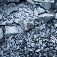
Silicon
Metalloid existing in various forms such as quartz, it is the second most abundant element on earth
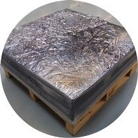
Ingot
Silicon melted in ingots and crystallized while reaching 1500°C
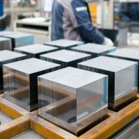
Brick
The ingots are cut into bricks before the polishing process and infrared inspection through silicon

Wafer
The bricks are cut into slices of
170 to 190 µm to produce LOW CARBON wafers
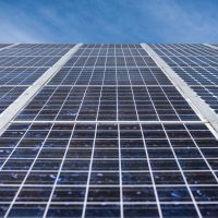
Cells & photovoltaic panels
Texturization of wafers, junction by phosphorus diffusion, contacts serigraphs.
Assembled by historical partners

Recycling
Photowatt is co-founder of SOREN, a solar panel is 96% recyclable.

Silicon
Metalloid existing in various forms such as quartz, it is the second most abundant element on earth

Ingot
Silicon melted in ingots and crystallized while reaching 1500°C

Brick
The ingots are cut into bricks before the polishing process and infrared inspection through silicon

Wafer
The bricks are cut into slices of
170 to 190 µm to produce LOW CARBON wafers

Cells & photovoltaic panels
Texturization of wafers, junction by phosphorus diffusion, contacts serigraphs.
Assembled by historical partners

Recycling
Photowatt is co-founder of SOREN, a solar panel is 96% recyclable

Recycling
Photowatt is co-founder of SOREN, a solar panel is 96% recyclable

Cells & photovoltaic panels
Texturization of wafers, junction by phosphorus diffusion, contacts serigraphs.
Assembled by historical partners

Wafer
The bricks are cut into slices of
170 to 190 µm to produce LOW CARBON wafers

Silicon
Metalloid existing in various forms such as quartz, it is the second most abundant element on earth

Ingot
Silicon melted in ingots and crystallized while reaching 1500°C

Brick
The ingots are cut into bricks before the polishing process and infrared inspection through silicon
Key figures

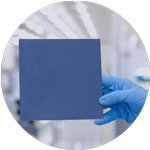


Our history
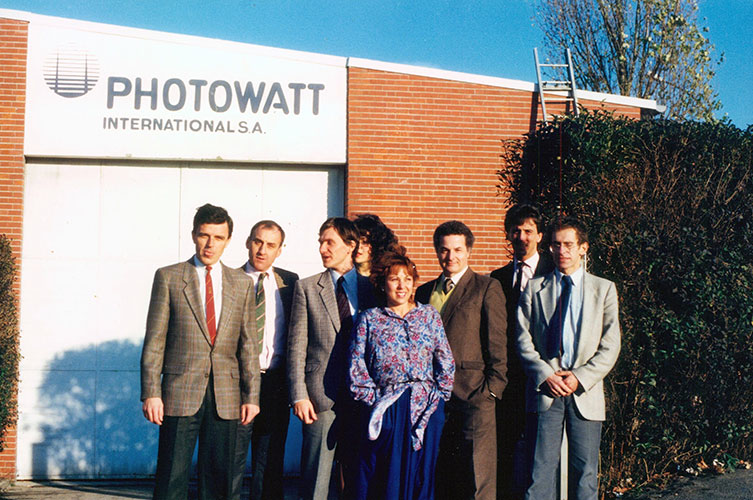
1979
Starting up as a research organization
Creation of Photowatt as a research center as a spin-off from Philipps (development of photovoltaic cells for satellites)
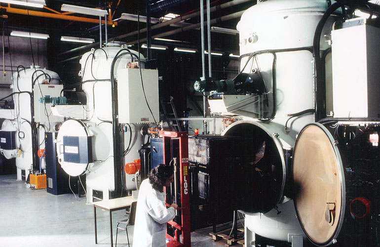
1984
Photowatt becomes producer
The company will broaden its vocation and take on an industrial dimension. Photowatt switches from 4-inch monocrystalline cells to multicrystalline silicon, thanks to the POLIX melting process that it has designed and industrialised itself. At the same time, it initiates the development of the first wire saws, used today by most manufacturers in the sector.
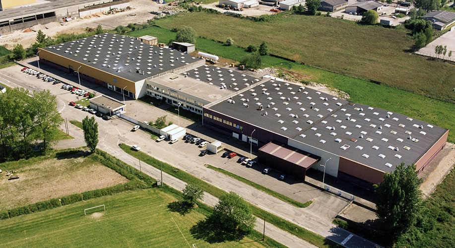
1990
Moving to Rhône-Alpes
The company moves to Bourgoin-Jallieu to expand and get closer to the industrial and research centres of Lyon and Grenoble in the Rhône-Alpes region. Photowatt remains a company with a production capacity of 3 MWp.
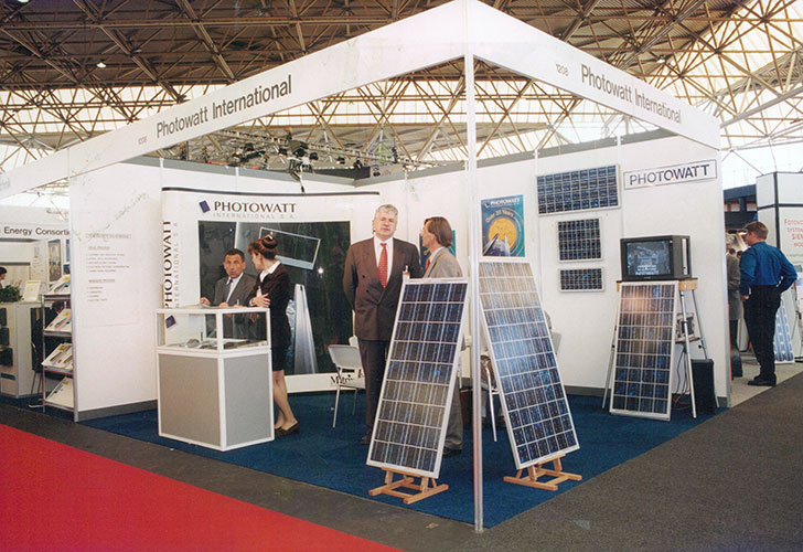
1997
New industrial dimension
The capacity is increased to 13 MWc, following the acquisition of the company by ATS. In 2001, Photowatt increases its wafer and cell manufacturing capacity and acquires a photovoltaic panel assembly line.
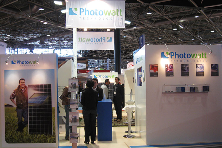
2000
Photowatt in the world's top 3
With Siemens and BP (Solarex) on Monocrystalline and Polycrystalline technologies.
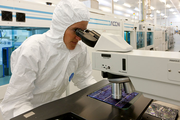
2007
Launch of PV Alliance
Launch of PV Alliance with EDF ENR and CEA within Photowatt to develop high efficiency cells.
2012
Integration into the EDF Group
Photowatt and PV Alliance become 100% subsidiaries of EDF Renewables.
2016
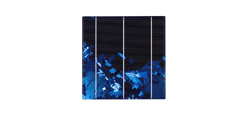
Crystal Advanced® Technology
Launch of photovoltaic panels and cells in Crystal Advanced® monolike technology, which offers high performance at low cost and a low carbon footprint.
2018
New industrial model
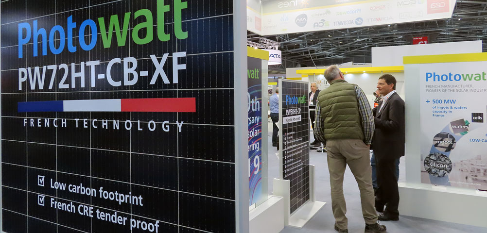
Increase in the production of low carbon ingots and wafers for the production of high performance monolike photovoltaic panel.